DSIT Get Hands-On in Semiconductor Processing
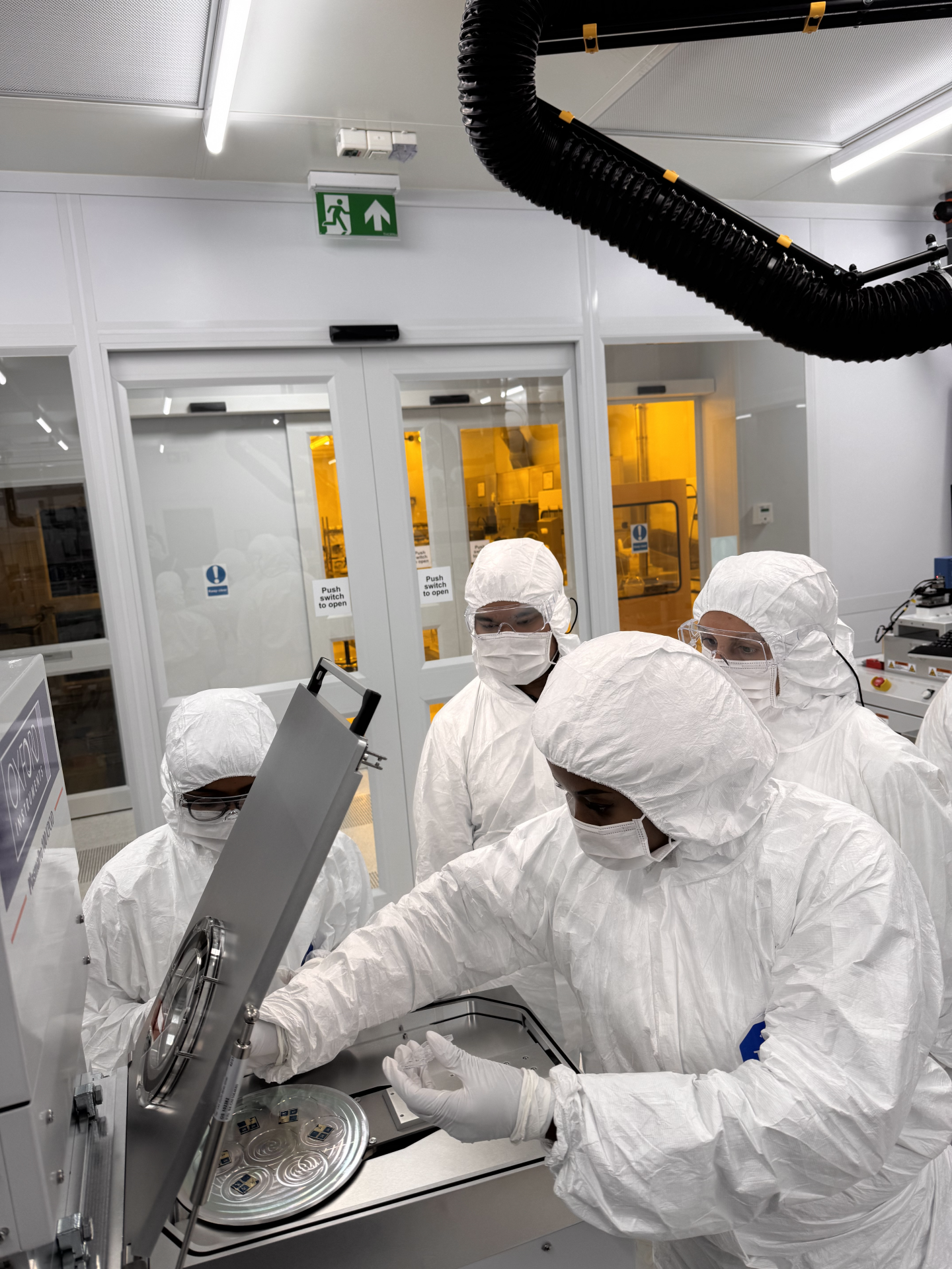
We were delighted to host a delegation from the Department for Science, Innovation and Technology (DSIT) in a unique, hands-on experience in semiconductor processing and device fabrication in the Leeds Nanotechnology Cleanroom. In their inaugural visit to a semiconductor fab, our six visitors experienced first-hand the precision, control and expertise that underpin every stage of micro- and nanofabrication.
We couldn’t, if we tried, match the depth and breadth of knowledge that you gifted us with.
Activities included:
The delegates were struck by the intricacy and discipline required to manufacture even a single layer of a device, and expressed admiration for the level of environmental control and technical knowledge needed to make it all possible. It was our pleasure to share the world of device fabrication with DSIT and to support a greater understanding of the infrastructure, skills, and innovation that drive UK research and development.